A couple of weeks ago I was browsing though a binder which contains part of my electronic circuits library. On of the pages from an old hobby and DIY magazine I stumbled on an interesting little circuit. The circuit was published in May 1976 and was intended to feed the small pocket calculators (aka mini-brains) that were just brought to the market. The first handheld calcualtors were thirsty devices and ran out of batteries far sooner then the current graphical calculators. The circuit in itself is nothing special but for me it started a quest to improve this simple circuit as much as possible.
Circuit Description
As can be seen the actual circuit is quit simple. R5 provides current for diodes D5 and D6. Thus at the anode of D6 there will be a constant voltage of circa ~1.4Volt. R4 provides the necessary current for transistor Q2. The base of transistor Q1 is connected to the circuit output via a (variable) voltage regulator R2 and R3.
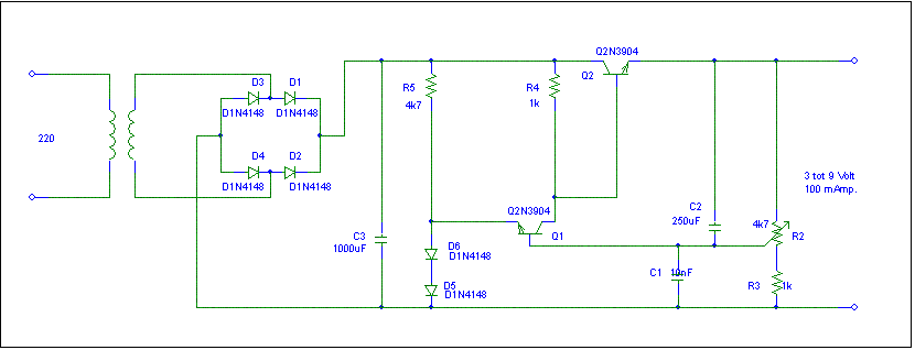
Output regulation works as follows: at the moment the circuit output rises the voltages at the basis of Q1 rises and Q1 will be forced to be opened more. Q1 will then draw more current through R4. Thus the voltage at the junction Q2 and R4 will lower and thus the output voltage.
Limitations
However, the simplicity of this circuit comes with limitations (there is no such thing as a free lunch). The two main limitations are 1) stability of the reference voltage at D5, D6 2)Feedback limitations
- The reference voltage of D5 and D6 is determined by the current through the diodes. The current through the diodes is determined by R5 as well as the unstabilized voltage after the diode bridge. Since the voltage is unstabilzed the current will vary and thus the reference voltage and the output voltage will follow.
- Feedback in this circuit is limited. The current through Q1 will vary with the output voltage. The large R4 the larger the swing in the voltage at Q2 and thus the regulation effect. However, R4 cannot be made too big because it also provides the base current for Q2...
| Input Voltage | Output Voltage | Rejection Ration | Output current | Output Voltage | Output resistance | |
| Figure 1 | 10V - 20V | 6.24V - 6.85V | 17x | 17mA - 110mA | 6.61V - 6.56V | 505mOhm |
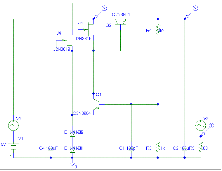
Improved circuit (1)
Although the issues describes above look quit different, both issues can be solved with the same technology.
With regards to the first issue there are two possible way to solve the issue 1) zenerdiodes or 2) constant current sources. The first option might seem to be most logical. However, I don't really like zenerdiodes for the fact that you never seem to have the right value at hand. In cases like this, it is often easier to create a more or less constant current through the diodes. With a constant current the voltage will alos be far more stable.
With regards to the second issue the resistor should supply enough current to drive transistor Q2 at all times, while at the same time be as large as possible to react on output voltage changes. So, actually you would like to have a large dynamic resistance. Even with a large voltage swing, the current variation should be kept relatively small this is exactly what a current source does..
| Input Voltage | Output Voltage | Rejection Ration | Output current | Output Voltage | Output resistance | |
| Figure 1 | 10V - 20V | 6.24V - 6.85V | 17x | 17mA - 110mA | 6.61V - 6.56V | 505mOhm |
| Figure 2 | 10V - 20V | 6.94V - 6.98V | 250x | 21mA - 118mA | 6.99V - 6.95V | 410mOhm |
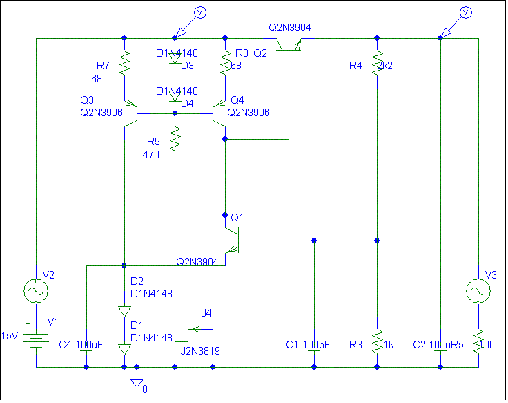
Improved circuit (2)
The circuit can be further imrpoved by using more stable current sources. Although FETs are easy to setup as a current source they are difficult to control because of the large tolrances and they are realivetly sensistive to drain-source voltage variations. In the next circuit circuit the current sources are swapped for common emittor current sources.
| Input Voltage | Output Voltage | Rejection Ration | Output current | Output Voltage | Output resistance | |
| Figure 1 | 10V - 20V | 6.24V - 6.85V | 17x | 17mA - 110mA | 6.61V - 6.56V | 505mOhm |
| Figure 2 | 10V - 20V | 6.94V - 6.98V | 250x | 21mA - 118mA | 6.99V - 6.95V | 410mOhm |
| Figure 3 | 10V - 20V | 6.88V - 6.89V | 625x | 20mA - 117mA | 6.90V - 6.86V | 400mOhm |
Literature
As inspiration to start this research the following sources were used
- Voeding voor minibreintjes, C.J. Both, Navijven, May 1976, page 44ff
- Cursus voor de radio-amateur (NL) Broken Link...
Have fun
Cor